A standard set of subcircuits is provided with the logic simulator for designing logic circuits using standard TTL chips. The TTL family of integrated circuits was introduced about 20 years ago by Texas Instruments. TTL stands for Transistor Transistor Logic, which signifies that two transistors are used to drive each output of each chip, one for pulling the output down to a low level, and one for pulling the output up to a high level. Chips made using TTL technology are faster than the older RTL (Resistor Transistor Logic) and DTL (Diode Transistor Logic) families of integrated circuits, and they consume more power than the MOS (Metal Oxide Semiconductor) technology used in most VLSI (Very Large Scale Integrated circuit) chips.
The TTL family has at least 6 subfamilies which offer different speed/power tradeoffs. These are summarized in the following table, where they are listed in roughly the order in which they were introduced:
|
family |
|
delay (ns) |
power (mW) |
|
basic |
|
10 |
10 |
|
low-power |
L |
35 |
1 |
|
Schottky |
S |
3 |
18 |
|
low-power Schottky |
LS |
9 |
2 |
|
advanced Schottky |
AS |
1.5 |
10 |
|
advanced low-power Schottky |
ALS |
4 |
1 |
The term Schottky refers to a technology for making faster transistors. It is interesting to note that, in each generation of the TTL family, the low power representative of that generation is about 3 times slower than the other member, but consumes about 1/10 the power. Today, the low-power Schottky subfamily is the most widely used member of the TTL family; chips from this family are available from a wide variety of manufacturers
All manufacturers of TTL chips use a common naming system, as
exemplified by the chip name ``SN74LS00''. The prefix SN indicates
that the chip was made by Texas Instruments; other manufacturers have
their own prefix codes, but if the remainder of the chip name
matches, the chips should perform exactly the same function.
Additional one letter codes may be added as prefixes or suffixes to
this code, for example, RSN indicates radiation hardened chips made
by Texas Instruments, and SNM indicates the use of quality control
procedures specified by the military specification MIL-STD-883. The
numeric code 74 indicates that the chip conforms to the requirements
of the civilian computer industry, being able to operate over a
temperature range of
![]() to
to
![]() C,
while the code 54 indicates the ability to operate over the more
extreme temperature range of
C,
while the code 54 indicates the ability to operate over the more
extreme temperature range of
![]() to
to
![]() C
required by many military and industrial applications. The letters LS
indicate which subfamily the chip belongs to. Finally, the last two
digits indicate the logical function performed by the chip.
C
required by many military and industrial applications. The letters LS
indicate which subfamily the chip belongs to. Finally, the last two
digits indicate the logical function performed by the chip.
Each Iowa Logic Specification Language TTL subcircuit description
corresponds to one standard chip, and these chips are packaged one
per file, in a form appropriate for inclusion using the use
statement. The actual file names of these circuits will depend on
your installation, but in general, the prefix indicating the
manufacturer and military rating will not be included in the name,
since it conveys nothing about the logical function of the chip. The
following circuit descriptions are currently available (listed in
numeric order):
The descriptions of these circuits are based on the details given in The TTL Data Book published by Texas Instruments. Equivalent data books are published by all of the major chip manufacturers such as Signetics and National Semiconductor. An effort has been made to make the simulated timings of these circuits match the documented timings of the corresponding chips. In general, the Data Book should be used as a source for information about these chips, while the information in the circuit descriptions should be considered secondary and subject to error.
Each circuit description in the TTL collection follows a common
scheme. The input and output pins of the chip have numeric names
corresponding to the pin numbers used for a dual-in-line package; for
example, for a 14 pin chip, these are p1, p2,
p3, and so on up to p14. For any given
chip, 2 of these pins are reserved for power (+5 volts) and ground (0
volts); these pins are not included in the chip descriptions, since
they serve electronic purposes below the level of abstraction with
which the logic simulator deals. The remaining pins are divided
between input and output connections.
For example, consider the SN74LS00 chip; this has 4 nand gates.
The inputs of the first nand gate are p1 and p2,
and its output is p3. The inputs of the second nand gate
are p4 and p5, and its output is p6.
The remaining nand gates are connected to p8 through
p13, and pins 7 and 14 are power and ground, and so are
not given names in the specification.
The input and output pins of the various chips are documented in the following sections, where the gates are listed in order by function. When a group of chips all have similar input and output connections, a diagram is given for only one of them, with the others listed below it. The diagrams on these pages are abbreviated and somewhat simplified compared with those in the data books; the data books should be used whenever an authoritative chip description is needed and these descriptions should only be used as a guide.
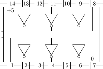
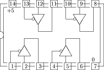
|
LS04 |
: |
Hex inverters. |
9.5ns |
![\begin{picture}% latex2html id marker 412(15,10)%% outline of 14 pin chip%... ...,0){2}{\circle{0.35}}\multiput(7.5,6.5)(6,0){2}{\oval(1.6,3.0)[t]}\end{picture}](indice-TTL_files/img11.gif)
|
LS00 |
: |
Quad 2-input nand gates. |
9.5ns |
|
|
LS08 |
: |
Quad 2-input and gates. |
9.0ns |
|
|
LS32 |
: |
Quad 2-input or gates. |
14ns |
|
|
LS86 |
: |
Quad exclusive or gates. |
10ns |
![\begin{picture}% latex2html id marker 495(15,10)%% outline of 14 pin chip%... ...,0){2}{\circle{0.35}}\multiput(3.5,6.5)(6,0){2}{\oval(1.6,3.0)[t]}\end{picture}](indice-TTL_files/img12.gif)
|
LS02 |
: |
Quad 2-input nor gates. |
10ns |
![\begin{picture}% latex2html id marker 578(15,10)%% outline of 14 pin chip%... ...,0){2}{\circle{0.35}}\multiput(5.5,6.5)(8,0){2}{\oval(1.6,3.0)[t]}\end{picture}](indice-TTL_files/img13.gif)
|
LS10 |
: |
Triple 3-input nand gates. |
9.5ns |
|
|
LS11 |
: |
Triple 3-input and gates. |
9.0ns |
|
|
LS27 |
: |
Triple 3-input nor gates. |
10ns |
![\begin{picture}% latex2html id marker 660(15,10)%% outline of 14 pin chip%... ...6}}\put(11.5,1.8){\circle{0.35}}\put(11.5,3.5){\oval(1.6,3.0)[b]}\end{picture}](indice-TTL_files/img14.gif)
|
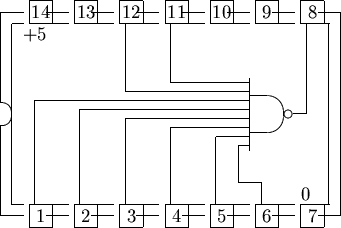
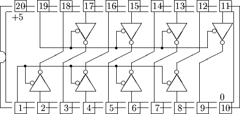
LS20 |
: |
Dual 4-input nand gates. |
9.5ns |
|
|
LS21 |
: |
Dual 4-input and gates. |
9.0ns |
|
LS30 |
: |
Single 8-input nand gates. |
10.5ns |
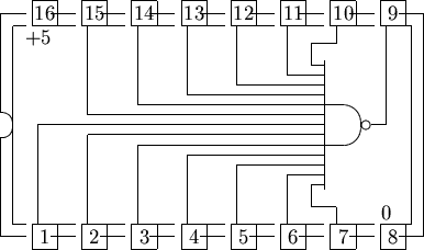
|
S133 |
: |
Single 13-input nand gates. |
6ns |
|
4c||inputs |
2coutput Y |
|
|
|
|
|
|
G |
S |
A |
B |
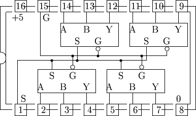
LS157 |
LS158 |
|
|
H |
x |
x |
x |
L |
H |
|
|
L |
L |
L |
x |
L |
H |
|
|
L |
L |
H |
x |
H |
L |
|
|
L |
H |
x |
L |
L |
H |
|
|
L |
H |
x |
H |
H |
L |
|
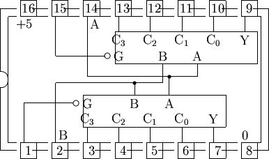
LS157 |
: |
Quad 2-line to 1-line multiplexers. |
9ns |
|
|
LS158 |
: |
Quad 2-line to 1-line inverting multiplexers. |
7ns |
|
3c||inputs |
2coutput Y |
|
|
|
|
|
G |
B |
A |
LS153 |
LS352 |
|
|
H |
x |
x |
L |
H |
|
|
L |
L |
L |
C0 |
|
|
|
L |
L |
H |
C1 |
|
|
|
L |
H |
L |
C2 |
|
|
|
L |
H |
H |
C3 |
|
|
LS153 |
: |
Dual 4-line to 1-line multiplexers. |
22ns |
|
|
LS352 |
: |
Dual 4-line to 1-line inverting multiplexers. |
22ns |
|
3c||inputs |
4coutputs |
|
|
|
|
|
||||
|
G |
B |
A |
Y0 |
Y1 |
Y2 |
Y3 |
||||
|
H |
x |
x |
H |
H |
H |
H |
||||
|
L |
L |
L |
L |
H |
H |
H |
||||
|
L |
L |
H |
H |
L |
H |
H |
||||
|
L |
H |
L |
H |
H |
L |
H |
||||
|
L |
H |
H |
H |
H |
H |
L |
|
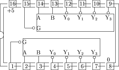
LS139 |
: |
Dual 2-line to 4-line decoders. |
22ns |
|
4c||inputs |
c@ c@ |
10coutputs |
|
c@ c@ c@ c@ c@ c@ c@ c@ |
|
|
D |
c@ c@ |
C |
B |
c@ c@ c@ c@ c@ c@ c@ c@ |
A |
|
L |
c@ c@ |
L |
L |
c@ c@ c@ c@ c@ c@ c@ c@ |
L |
|
L |
c@ c@ |
L |
L |
c@ c@ c@ c@ c@ c@ c@ c@ |
H |
|
L |
c@ c@ |
L |
H |
c@ c@ c@ c@ c@ c@ c@ c@ |
L |
|
L |
c@ c@ |
L |
H |
c@ c@ c@ c@ c@ c@ c@ c@ |
H |
|
L |
c@ c@ |
H |
L |
c@ c@ c@ c@ c@ c@ c@ c@ |
L |
|
L |
c@ c@ |
H |
L |
c@ c@ c@ c@ c@ c@ c@ c@ |
H |
|
L |
c@ c@ |
H |
H |
c@ c@ c@ c@ c@ c@ c@ c@ |
L |
|
L |
c@ c@ |
H |
H |
c@ c@ c@ c@ c@ c@ c@ c@ |
H |
|
H |
c@ c@ |
L |
L |
c@ c@ c@ c@ c@ c@ c@ c@ |
L |
|
H |
c@ c@ |
L |
L |
c@ c@ c@ c@ c@ c@ c@ c@ |
H |
|
H |
c@ c@ |
L |
H |
c@ c@ c@ c@ c@ c@ c@ c@ |
x |
|
H |
c@ c@ |
H |
x |
c@ c@ c@ c@ c@ c@ c@ c@ |
x |
|
LS42 |
: |
BCD-to-decimal or binary-to-octal decoder. |
17ns |
To use the LS42 as a binary-to-octal decoder, ignore outputs Y8 and Y9, apply the binary input to C, B and A, and use input D as a negative-logic enable signal.
|
3c||inputs |
2coutputs |
|
|
|
|||
|
A |
B |
|
|
|
|||
|
L |
L |
L |
L |
L |
|||
|
L |
L |
H |
H |
L |
|||
|
L |
H |
L |
H |
L |
|||
|
L |
H |
H |
L |
H |
|||
|
H |
L |
L |
H |
L |
|||
|
H |
L |
H |
L |
H |
|||
|
H |
H |
L |
L |
H |
|||
|
H |
H |
H |
H |
H |
|
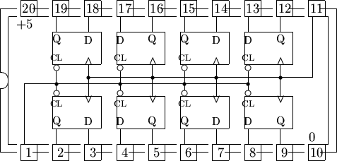
LS183 |
: |
Dual full adders. |
15ns |
|
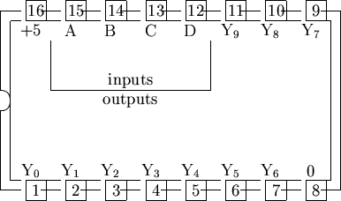
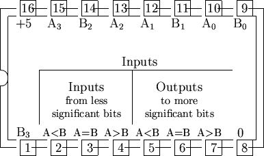
LS85 |
: |
4-bit binary magnitude comparators |
24ns |
In A and B, the two words to be compared, bit 0 is the least significant bit, and positive logic is used. The <, =, and > inputs to the least significant end of a chain of comparators should be L, H, and L respectively; the outputs from the most significant end are positive logic.
![\begin{picture}% latex2html id marker 1425(21,10)%% outline of 20 pin chip%... ...\makebox(0,1)[l]{outputs}}\put(12.5,4){\makebox(0,1)[r]{inputs}}%\end{picture}](indice-TTL_files/img30.gif)
|
3c||select |
output |
|
|
||
|
S2 |
S1 |
S0 |
F |
||
|
L |
L |
L |
0000 |
||
|
L |
L |
H |
B minus A |
||
|
L |
H |
L |
A minus B |
||
|
L |
H |
H |
A plus B |
||
|
H |
L |
L |
A xor B |
||
|
H |
L |
H |
A or B |
||
|
H |
H |
L |
A and B |
||
|
H |
H |
H |
1111 |
|
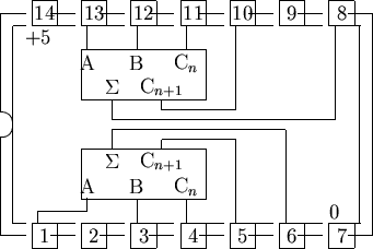
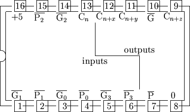
LS381A |
: |
4-bit ALU slice with look-ahead carry outputs. |
17ns |
|
|
LS382 |
: |
4-bit ALU slice with ripple carry outputs. |
17ns |
In A and B, the two operands, as well as in F, the result, bit 0 is the least significant bit, and positive logic is used. The delay given is from A and B to F; the function select input S must typically be set up at least 38ns prior to examining the outputs, while the carry input Cn typically takes only 16ns to reach the outputs.
The LS381A produces
![]() and
and
![]() outputs on pins 14 and 13 which can be used as inputs to S182 chips
for look-ahead carry generation. When
outputs on pins 14 and 13 which can be used as inputs to S182 chips
for look-ahead carry generation. When
![]() is low, the 4-bit slice will propagate a carry, while when
is low, the 4-bit slice will propagate a carry, while when
![]() is low, the 4-bit slice will generate a carry.
is low, the 4-bit slice will generate a carry.
The LS382 produces Cn+4
on pin 14, allowing ripple carry between 4-bit slices. The OVR output
on pin 13 indicates signed two's complement overflow; effectively, it
indicates that
![]() .
.
Note that when using either ALU to perform subtraction, both the carry in and carry out signals indicate the absence of a borrow. Thus, C0 (the carry in to the least significant bit) should be 1 during subtraction.
|
S182 |
: |
Look-ahead carry generators. |
6ns |
The S182 look-ahead carry generator can provide look-ahead carry propagation for as many as 4 ALUs such as the LS381A, and a tree of 5 S182 chips will serve to provide fast carry across 16 LS381A ALUs, allowing 64 bit arithmetic operations in typically 45ns (from data inputs to data outputs, assuming that the ALU function has been selected in advance).
For both inputs and outputs,
![]() will be low if an ALU or group of ALUs will propagate a carry, and
will be low if an ALU or group of ALUs will propagate a carry, and
![]() will be low if an ALU or group of ALUs will generate a carry.
will be low if an ALU or group of ALUs will generate a carry.
![]() through
through
![]() and
and
![]() through
through
![]() are inputs from ALUs or groups of ALUs, with increasing subscripts
indicating more significant ALUs.
are inputs from ALUs or groups of ALUs, with increasing subscripts
indicating more significant ALUs.
![]() and
and
![]() are outputs from this group of ALUs to higher levels in the tree.
are outputs from this group of ALUs to higher levels in the tree.
The Cn input (positive logic)
indicates carry in to this group of ALUs, and it should be the same
as the carry in to the least significant ALU in the group. Cn+x,
Cn+y and Cn+z
are outputs to the 3 more significant ALU's in the group, in order of
increasing significance. These do not depend on
![]() or
or
![]() ,
so the most significant ALU used for a full word operation need not
produce look-ahead signals.
,
so the most significant ALU used for a full word operation need not
produce look-ahead signals.
|
LS125A |
: |
Quadruple non-inverting three-state buffers. |
9ns |
|
LS240 |
: |
Octal inverting three-state buffers. |
10.5ns |
|
|
LS244 |
: |
Octal non-inverting three-state buffers. |
12ns |
|
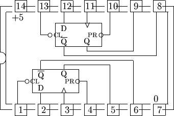
LS74A |
: |
Dual D positive-edge-triggered flipflops. |
25ns |
|
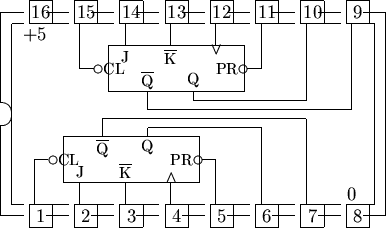
LS109A |
: |
Dual J- |
24ns |
|
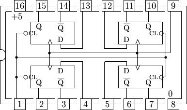
LS175 |
: |
Quad D positive-edge-triggered flipflops. |
20ns |
|
LS174 |
: |
Hex D positive-edge-triggered flipflops. |
20ns |
|
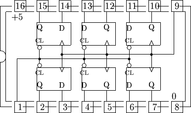
LS273 |
: |
Octal D flipflops with clear. |
18ns |
|
|
LS374 |
: |
Octal D flipflops with three-state outputs. |
20ns |
The clear input CL to each flipflop on the LS273 is replaced on the LS374 by an output-enable input called OE. Both CL and OE use negative logic, and all of these flipflops are positive edge triggered.
|
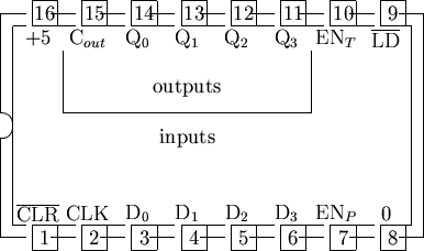
LS161A |
: |
Synchronous 4-bit binary counter. |
14ns |
The LS161A binary counter has a positive edge
triggered clock input CLK, and a negative logic asynchronous clear
input
![]() .The
value stored in the counter is continuously presented on the Q
outputs (
.The
value stored in the counter is continuously presented on the Q
outputs (![]() is least significant, positive logic is used).
is least significant, positive logic is used).
When
![]() is held low, data from the D inputs will be loaded into the counter
when it is clocked. When
is held low, data from the D inputs will be loaded into the counter
when it is clocked. When
![]() ,
,
![]() and
and
![]() are all held high, the counter will increment when clocked. Holding
either
are all held high, the counter will increment when clocked. Holding
either
![]() or
or
![]() inputs low will inhibit counting. The
inputs low will inhibit counting. The
![]() output indicates that the counter holds the value 1111 and the
output indicates that the counter holds the value 1111 and the
![]() input is high.
input is high.
To build high precision synchronous counters, wire
the
![]() output of each stage to the
output of each stage to the
![]() input of the next more significant stage, and wire the CLK,
input of the next more significant stage, and wire the CLK,
![]() ,
,
![]() and
and
![]() inputs in parallel across all stages.
inputs in parallel across all stages.
|
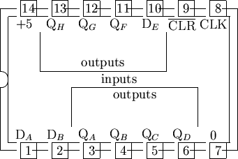
LS164 |
: |
8-bit serial to parallel shift register. |
28ns |
The LS164 shift register has a positive edge
triggered clock CLK and a negative logic asynchronous clear
![]() .All
8 bits stored in the register are continuously displayed on the data
outputs
.All
8 bits stored in the register are continuously displayed on the data
outputs
![]() to
to
![]() ,
where
,
where
![]() was the most recent value shifted into the register.
was the most recent value shifted into the register.
The serial data inputs
![]() and
and
![]() are anded together; both must be high to shift a high into the
register; either or both may be low to shift a low into the register.
are anded together; both must be high to shift a high into the
register; either or both may be low to shift a low into the register.
To make a longer shift register, wire the
![]() output of one stage to the serial data inputs of the next stage, and
wire all clock and clear inputs in parallel across all stages.
output of one stage to the serial data inputs of the next stage, and
wire all clock and clear inputs in parallel across all stages.
|
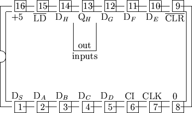
LS166 |
: |
8-bit parallel to serial shift register. |
28ns |
The LS166 shift register has a positive edge
triggered clock CLK and a positive logic clock-inhibit input CI. CI
should not change from low to high except when CLK is already high.
![]() is a negative logic asynchronous clear. The value stored in the 8th
bit of the register is continuously presented on the output
is a negative logic asynchronous clear. The value stored in the 8th
bit of the register is continuously presented on the output
![]() .
.
When
![]() is held low, data from the inputs
is held low, data from the inputs
![]() to
to
![]() will be loaded into the register when it is clocked. When
will be loaded into the register when it is clocked. When
![]() is held high, the register will shift when it is clocked, with new
data entering stage A of the register from the serial data input
is held high, the register will shift when it is clocked, with new
data entering stage A of the register from the serial data input
![]() .
.
Longer shift registers can be made by chaining the
![]() output of one stage to the
output of one stage to the
![]() input of the next, and connecting the CLK, CI,
input of the next, and connecting the CLK, CI,
![]() ,
and
,
and
![]() inputs in parallel across all stages.
inputs in parallel across all stages.
Pagina original en
http://www.cs.uiowa.edu/~jones/logicsim/man/node5.html